Low Power, High Reliability, Robust Antifuse FPGAs
Antifuse FPGAs ideal for battery powered, High reliability, instant-on, Aerospace and Military applications
Trusted, Flexible, Reliable
Over three decades of service to mission-critical applications
Over three decades of service to mission-critical applications
Non-volatile architecture for the highest reliability applications
Zero boot-up time solution for time-sensitive communications and munitions projects
Five Global Clock Networks with Configurable Clock Managers
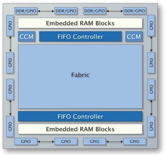
Dual-port embedded SRAM, Native DDR Support and dedicated FIFO logic
Anti-fuse design means lowest power FPGAs
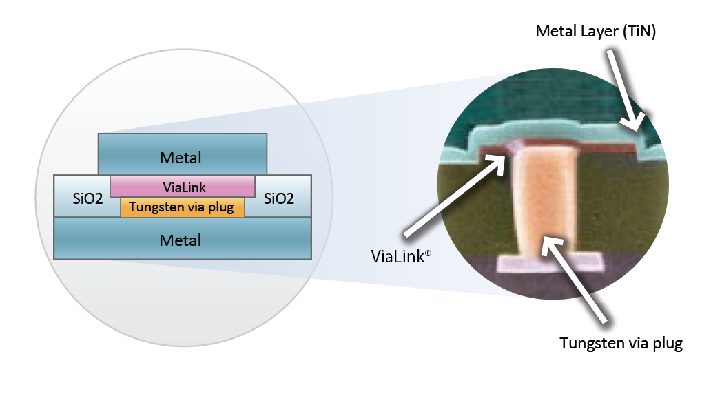
Compact ViaLink fabric yields small die sizes and package footprints
Available factory programming with traceable, unique part identification
No separate memory chip minimizes BOM, PCB area, and cost
Non-volatile FPGAs are considered simple logic elements easing aerospace or military approval
Fast prototyping at your desk, short lead times for production
Improved battery life and heat dissipation
30-year history supplying >50M devices to a variety of industries


The PolarPro II series consists of a single 864 logic cell part available in three narrow-pitch packages. It was optimized for low-power, small footprint applications and manufactured in a 0.18um, six-layer metal CMOS process.
| Features | QL2P150 | |
|---|---|---|
| Max Gates | 150,000 | |
| Logic Cells | 864 | |
| RAM Modules | 8 | |
| FIFO Controllers | 8 | |
| RAM bits | 27,648 | |
| CCMs | 1 | |
| Max I/O per Package | 144 VFBGA (0.4 mm pitch) | 103 |
| 121 TFBGA (0.5 mm pitch) | 81 | |
| 64 WLCSP (0.4 mm pitch) | 41 | |
For product availability, please contact sales@quicklogic.com before starting your design.
The PolarPro series consists of six devices with a range of 512 to 7,680 logic cells available in up to six TFBGA, TQFP, and LBGA packages. It was optimized for low-power applications in a variety of markets and manufactured in a 0.18um, six-layer metal CMOS process.
| Features | QL1P075 | QL1P100 | QL1P200 | QL1P300 | QLP600 | QLP1000 | ||
|---|---|---|---|---|---|---|---|---|
| Max Gates | 75,000 | 100,000 | 200,000 | 300,000 | 600,000 | 1,000,000 | ||
| Logic Cells | 512 | 640 | 1,536 | 1,920 | 4,224 | 7,680 | ||
| Max I/O | 168 | 184 | 238 | 238 | 232 | 244 | ||
| RAM Modules | 8 | 8 | 12 | 12 | 24 | 24 | ||
| FIFO Controllers | 8 | 8 | 12 | 12 | 24 | 24 | ||
| RAM bits | 36,864 | 36,864 | 55,296 | 55,296 | 221,184 | 221,184 | ||
| CCM(s) | 2ª | 2ª | 2 | 2ª | 2 | 2 | ||
| Packages | WLCSP (0.5 mm) | 99 | - | - | - | - | - | |
| TFBGA (0.5 mm) | - | 121 | - | - | - | - | ||
| TFBGA (0.5 mm) | 132 | 132 | 132 | 132 | - | - | ||
| TQFP (0.5 mm) | 144 | 144 | - | - | - | - | ||
| TFBGA (0.8 mm) | 196 | 196 | - | - | - | - | ||
| LBGA (1.0 mm) | 256 | 256 | 256,324 | 256, 324 | 324 | 324 |
For product availability, please contact sales@quicklogic.com before starting your design.
The Eclipse II series consists of five devices with a range of 128 to 1,536 logic cells available in up to eight TFBGA, TQFP, VQFP, PQFP, PBGA and LFBGA packages. It features Embedded Computational Units (ECUs) in the larger devices and was optimized for smaller array-size, low-power applications in a variety of markets and manufactured in a 0.18um, six-layer metal CMOS process.
| QL8025 | QL8050 | QL8150 | QL8250 | QL8325 | 47,052 | 63,840 | 188,946 | 248,160 | 320,640 |
|---|---|---|---|---|---|---|
| Logic Array | 16 X 8 | 16 X 16 | 32 X 20 | 40 X 24 | 48 X 32 | |
| Logic Cells | 128 | 256 | 640 | 960 | 1,536 | |
| Max Flip-Flops | 532 | 884 | 1,709 | 2,670 | 4,002 | |
| Max I/O | 92 | 124 | 165 | 250 | 310 | |
| RAM Modules | 4 | 4 | 16 | 20 | 24 | |
| RAM Bits | 9,216 | 9,216 | 36,864 | 46,100 | 55,300 | |
| PLLs | - | - | - | 4 | 4 | |
| ECUs | - | - | - | 10 | 12 | |
| Packages | VQFP | 100 | 100 | - | - | - |
| TFBGA (0.5 mm) | - | 101 | - | - | - | |
| TQFP | 144 | 144 | 144 | - | - | |
| TFBGA (0.8 mm) | 196 | 196 | 196 | - | - | |
| TFBGA (0.5 mm) | - | 101 | 196 | - | - | |
| PQFP | - | - | 208 | 208 | 208 | |
| LFBGA (0.8 mm) | - | - | 280 | 280 | 280 | |
| PBGA (1.0 mm) | - | - | - | 484 | 484 | |
For product availability, please contact sales@quicklogic.com before starting your design.
The Eclipse Plus features the same technology and array sizes as the Eclipse series but adds Embedded Computational Units (ECUs), DSP blocks which speed up signal processing tasks.
| QL7100 | QL7120 | QL7160 | QL7180 | ||
|---|---|---|---|---|---|
| Max Gates | 292,160 | 373,440 | 558,464 | 662,208 | |
| Logic Array | 40 X 24 | 48 x 32 | 64 x 48 | 72x56 | |
| Logic Cells | 960 | 1,536 | 3,072 | 4,032 | |
| Max Flip-Flops | 2,670 | 3,692 | 7,185 | 9,105 | |
| Max I/O | 250 | 310 | 347 | 347 | |
| RAM Modules | 20 | 24 | 32 | 36 | |
| RAM Bits | 46,100 | 55,300 | 73,700 | 82,900 | |
| PLLs | 4 | 4 | 4 | 4 | |
| ECUs | 10 | 12 | 16 | 18 | |
| Packages | PQFP (0.5 mm) | 208 | 208 | - | - |
| LFBGA (0.8 mm) | 280 | 280 | 280 | 280 | |
| PBGA (1.0 mm) | 484 | 484 | 484 | 484 | |
| PBGA (1.27 mm) | - | - | 516 | 516 | |
The Eclipse series consists of four devices with a range of 960 to 4,032 logic cells available in up to four PQFP, PBGA,FPBGA and LFBGA packages. It was optimized for low-power applications in a variety of markets and manufactured in a 0.25um, five-layer metal CMOS process.
| QL6250 | QL6325 | QL6500 | QL6600 | ||
| Max Gates | 248,160 | 320,640 | 488,064 | 583,008 | |
| Logic Array | 40x24 | 48x32 | 64x48 | 72x56 | |
| Logic Cells | 960 | 1,536 | 3,072 | 4,032 | |
| Max Flip-Flops | 2,670 | 4,002 | 7,185 | 9,105 | |
| Max I/O | 250 | 310 | 347 | 347 | |
| RAM Modules | 20 | 24 | 32 | 36 | |
| RAM bits | 46,100 | 55,300 | 73,700 | 82,900 | |
| Packages | PQFP | 208 | 208 | - | - |
| PBGA (1.27 mm) | - | - | 516 | 516 | |
| FPBGA (1.0 mm) | 484 | 484 | 484 | 484 | |
| LFBGA (0.8 mm) | 280 | 280 | 280 | 280 | |
The QuickRAM series consists of five devices with a range of 160 to 1,584 logic cells available in up to five PLCC, TQFP, PQFP, PBGA and CQFP packages. The architecture and array sizes are the same as the five largest pASIC 3 devices, but also include block RAM. It was optimized for high speed, low-power applications in a variety of markets and manufactured in a 0.35um, four-layer metal CMOS process.
| QL4009 | QL4016 | QL4036 | QL4058 | QL4090 | ||
|---|---|---|---|---|---|---|
| Max Gates | 44,964 | 61,820 | 97,128 | 131,328 | 176,608 | |
| Logic Array | 16 X 16 | 20x 16 | 28 x 24 | 36 x 28 | 44 x 36 | |
| Logic Cells | 160 | 320 | 672 | 1,008 | 1,584 | |
| Max Flip-Flops | 242 | 438 | 876 | 1,260 | 1,900 | |
| Max I/O | 74 | 110 | 196 | 244 | 308 | |
| RAM Modules | 8 | 10 | 14 | 18 | 22 | |
| RAM Bits | 9,216 | 11,520 | 16,128 | 20,736 | 25,334 | |
| Packages | PLCC | 68/84 | 84 | - | - | - |
| TQFP | 100 | 100/144 | 144 | - | - | |
| PQFP | - | - | 208 | 208/240 | 208/240 | |
| PBGA | - | - | 256 | 456 | 456 | |
| CQFP | - | 100 | - | - | 208 | |
The pASIC 3 series consists of six devices with a range of 96 to 1,584 logic cells available in up to seven PLCC, TQFP, PQFP, and PBGA packages. It was optimized for high speed, low-power applications in a variety of markets and manufactured in a 0.35um, four-layer metal CMOS process.
| QL3004 | QL3004E | QL3006 | QL3012 | QL3025 | QL3040 | QL3060 | ||
|---|---|---|---|---|---|---|---|---|
| Max Gates | 5,188 | 5,188 | 8,008 | 15,740 | 32,616 | 48,384 | 75,232 | |
| Logic Array | 8 X 12 | 8 X 12 | 10 X 16 | 20 X 16 | 28 X 24 | 36 X 28 | 44 X 36 | |
| Logic Cells | 96 | 96 | 160 | 320 | 672 | 1,008 | 1,584 | |
| Max Flip-Flops | 178 | 178 | 322 | 438 | 876 | 1,260 | 1,900 | |
| Max I/O | 74 | 74 | 74 | 110 | 196 | 244 | 308 | |
| Packages | PLCC | 68 | 68 | 68 | - | - | - | - |
| PLCC | 84 | 84 | 84 | 84 | - | - | - | |
| TQFP | 100 | 100 | 100 | 100 | 100 | - | - | |
| TQFP | - | - | - | 144 | 144 | - | - | |
| PQFP | - | - | - | - | 208 | 208 | 208 | |
| PBGA | - | - | - | - | 256 | - | - | |
| PBGA | - | - | - | - | - | 456 | 456 | |